While designing a sensor breakout PCB I decided it would be useful to include power input protection in the form of reverse voltage protection and overvoltage protection. I designed the circuit shown below, a combination along with slight modification of two circuits I found online.

The reverse polarity protection circuit is from a video by Afrotechmods, a similar circuit can be found in the TI app note SLVA139. The overvoltage protection circuit is a modification of the circuit of Figure 1 in the Maxim app note 760. Since I was using a P-channel MOSFET in the polarity protection circuit, it seemed best to try to modify the Maxim app note to use the same P-channel MOSFET instead of a bipolar transistor thereby reducing the part count. Only an additional Zener diode, D1, was needed to prevent the gate of the P-channel MOSFET from exceeding the ±20V maximum rating. I original omitted this Zener diode and it was not until I was characterizing the circuit that I thought about needing to protect the gate of both P-channel MOSFETs.
The circuit is designed for ±40Vdc maximum input voltage at a load current of 2A, this is limited by the maximum voltage rating of the P-channel MOSFETs. For larger input voltages and current loads, higher rated P-channel MOSFETs will need to be used. The overvoltage protection will cut off power at about 28Vdc, this voltage is set using Zener diode D3. R3 sets the current flow through D2, a maximum of 5mA at 40V. Similarly resistor R4 limits the current through D1 and the maximum current through Q3 when it is fully saturated. Resistor R1 sets the current flowing through D3 and into the base of Q3.
I was also planning on implementing overcurrent protection and happened to catch a video by Jeri Ellsworth outlining such a circuit using discrete components. I could never get the circuit working correctly so I have omitted overcurrent protection for now.
Overvoltage Protection
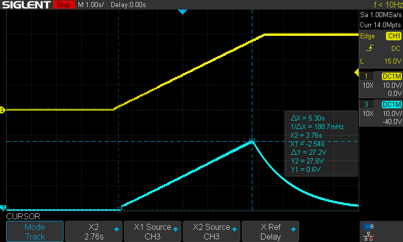
To test the overvoltage protection functionality of this circuit I setup a programmable power supply to ramp voltage from 0 to 30Vdc. I used an oscilloscope to capture the input and output voltage. The oscilloscope was setup to trigger at 15V in single shot capture mode. The below capture was without an output load. The overvoltage protection activates at 27.8V.
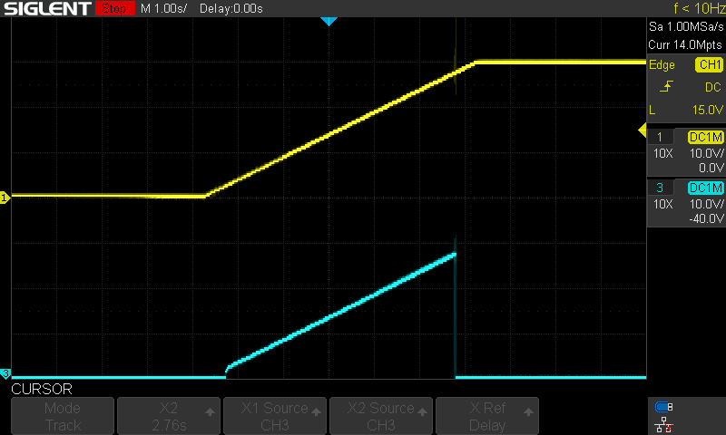
I then added a 0.5A load to the output of the circuit.
There appears to be some instability of the output voltage where the overvoltage protection triggers. Zooming in it is possible to see that the output voltage will oscillate while the input voltage is close to the overvoltage trigger point.
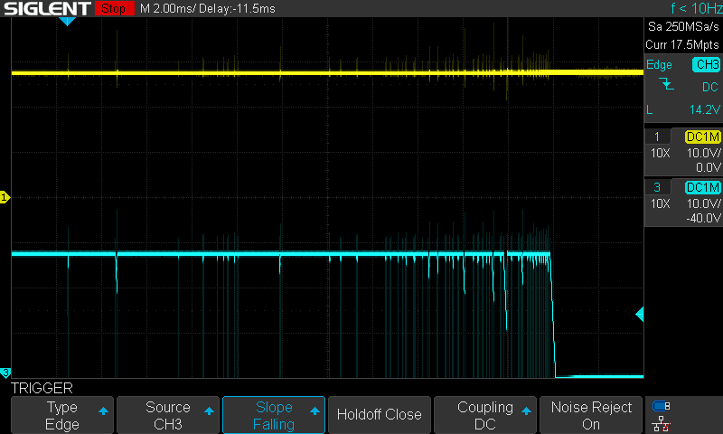
The overvoltage function of this circuit does work and triggers at 27.8V. The oscillation of the output voltage when connected to a load around this overvoltage trigger point is an undesirable part of this circuit. For future use I will have to find a way to add hysteresis to the circuit or make it latching when an overvoltage condition occurs.
Circuit Characterization
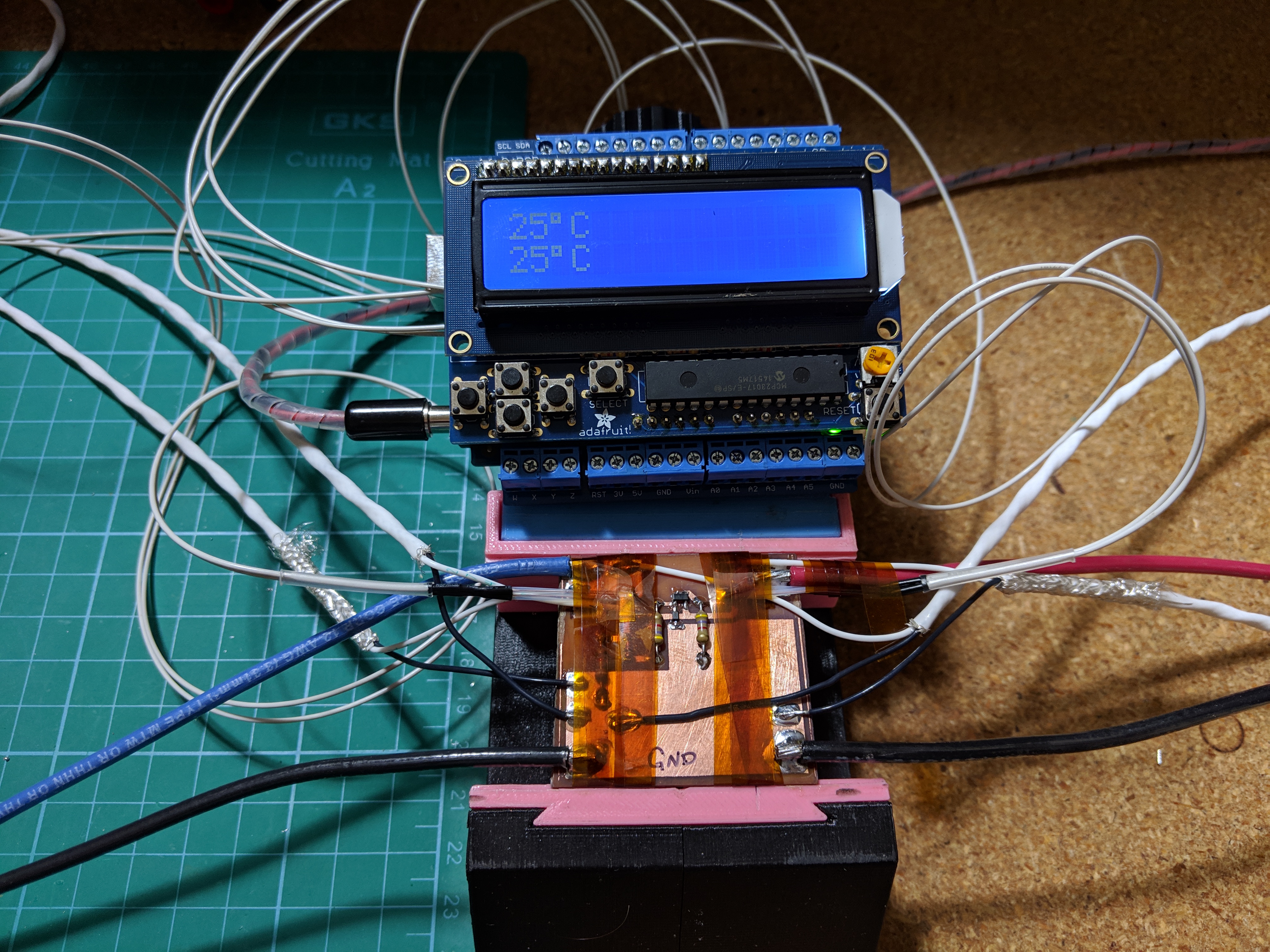
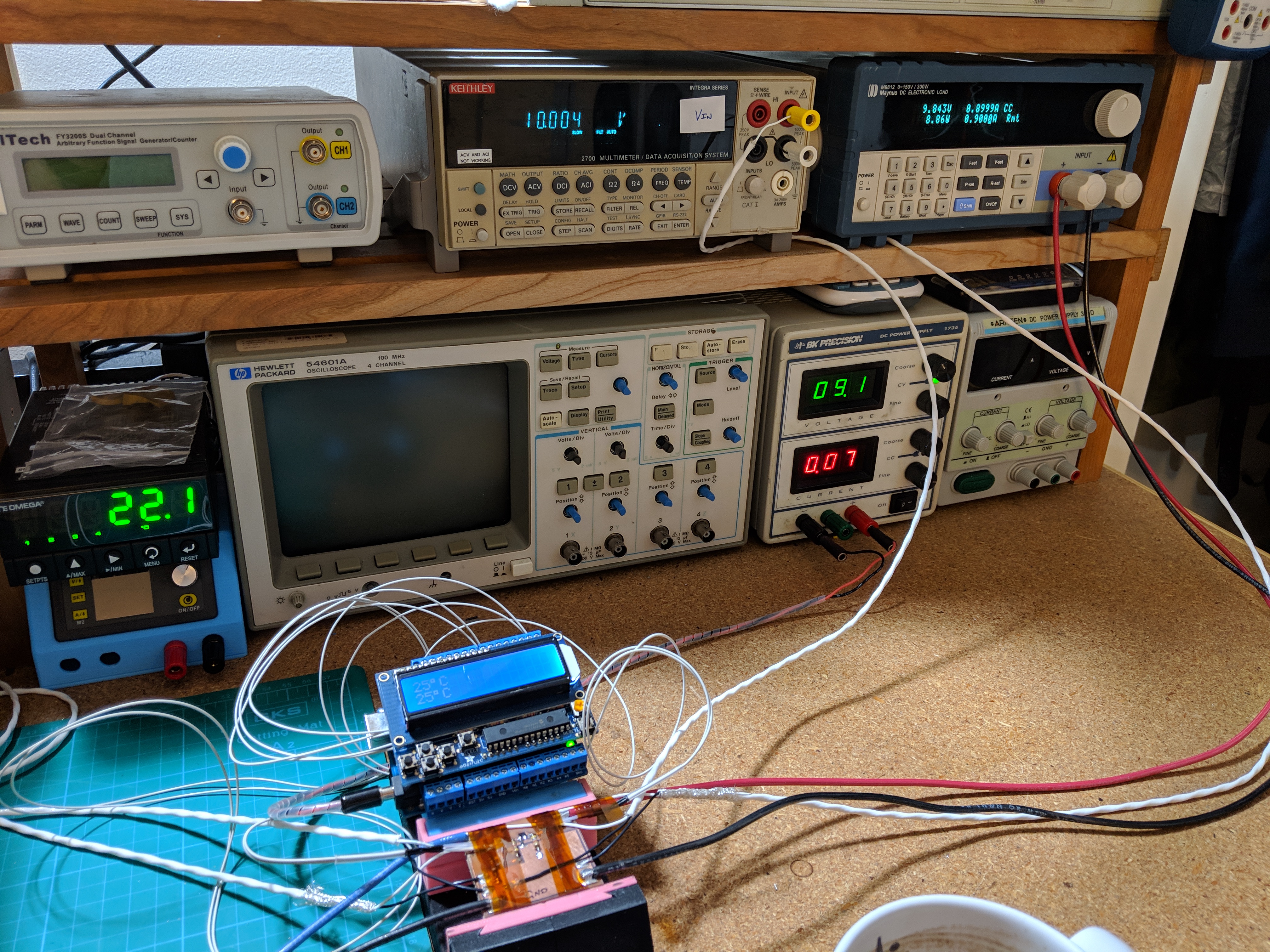
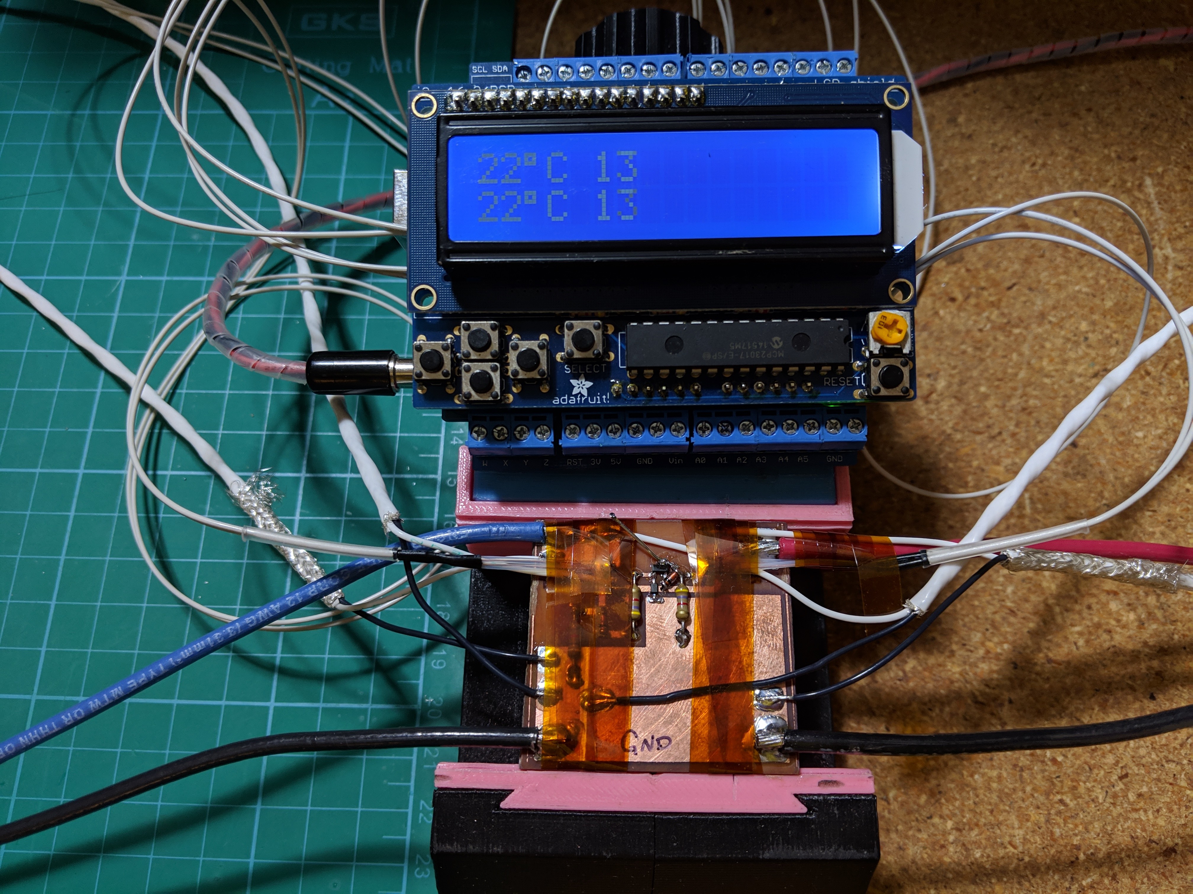
Below are characterization plots of one assembled circuit built on a home etched PCB. These curves are only valid if using the exact components and values as shown in the schematic. Also this data is from only one circuit so it may vary greatly from circuit to circuit.
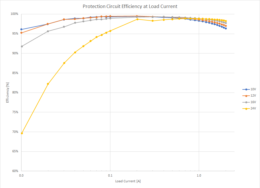
The circuit is most efficient at 10-12VDC input voltage with 50mA to 500mA of load current. The application I intend to use this circuit on will operate most of the time at this input voltage and load current.
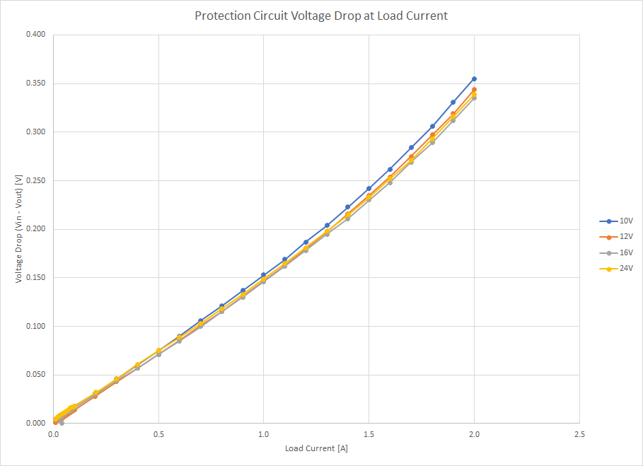
The voltage drop is similar regardless of input voltage. Even at a full load current of 2A the drop is far less than a standard diode drop of 0.7V and within the voltage drop of a Schottky diode. Again this works well for my intended application.
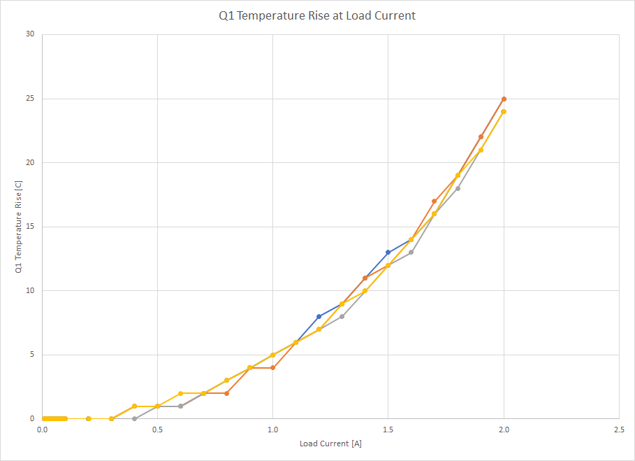
At a load current of 1A or less the temperature of Q1 rises a maximum of 5°C. Load currents exceeding 1A cause an accelerated rise in temperature but remains below a 25°C temperature rise. Equipment failure during testing rendered the measurements of Q2 useless (coding error, aghh!). I went back and measured the temperature rise of Q2 at an input voltage of 10V and 24V with a load current of 2A and the temperature rise of Q2 was about 3°C lower than Q1. Therefor the temperature of Q1 and Q2 are close enough to similar for my purposes. In application I will be sure to add sufficient copper pours around these P-channel MOSFETs to act as heat sinking, maybe that can reduce the temperature rise by a few degrees.
A spreadsheet of my measurements can be found in the GitHub repository for this project here: DMP4065S_Polarity_Overvoltage_Protection.xlsx
Future Testing
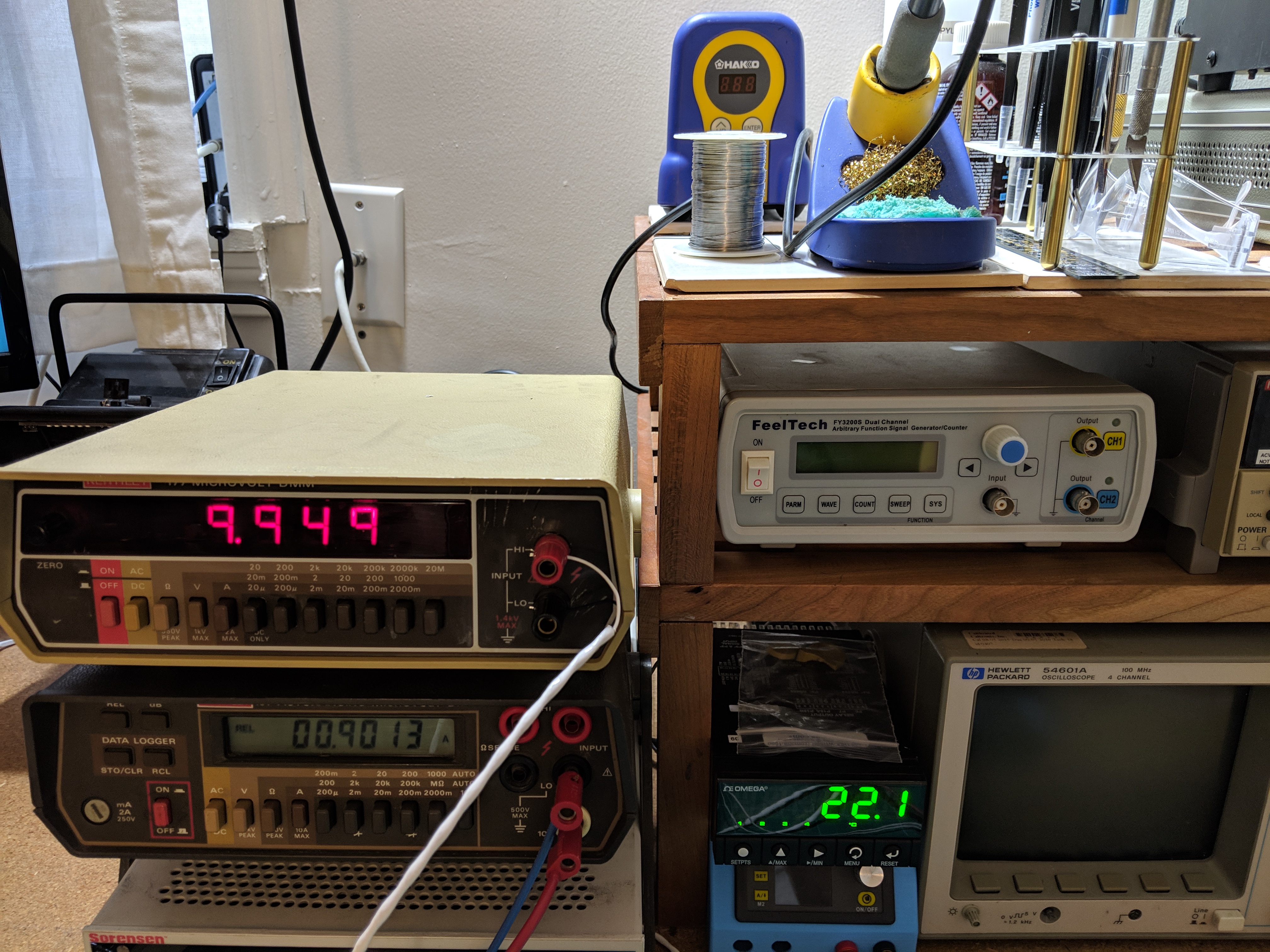
I would like to explore this circuit with some more testing in the future such as trying different P-channel MOSFETs and resistor values. I would also like to be able to measure more of the circuit than just the input and output parameters, I have picked up some more meters to do this but I first have to fix them. I also want to automate the measurements since it took a full day to collect the data for the three characterization plots above. I have my eye on a programmable power supply that should assist with this task. This also means that the new meters I picked up have to be modified for digital data collection. Sounds like a blog post for another day.
Most of the above was written in January 2019 and has stayed as a draft for reasons unknown to me. I did end up using a version of this circuit in a project for work and found it adequate for the needs of that particular application. I want to have this circuit as something that I put into most of my projects. I already use the reverse protection circuit in any project that the user can easily swap voltage polarity but also having overvoltage protection using discrete components would be great. I have seen and experimented with eFuses but have found that they can be expensive or limited in overvoltage adjustment.
Thanks for reading to the end. All design files, schematic, data, and more is available in the GitHub repository for you to use as you wish. If you find any errors or have any improvements please leave a comment.
